
Nearly all modern PCBs are designed with the help of EDA software, but not all of them. [ALTco] shows us the process of plotting out a board the old-fashioned way — by hand.
Back in the day, drawing out the traces on a PCB lead to beautiful, smooth lines that [ALTco] wanted to imitate. But first, he needed to figure out how the rest of the fabrication process worked. He starts by just experimenting, both with the “resist” markers and paint, and the etching compound. Things rarely work first-try, and neither did his home-made etchant. So then it was time to buy some ferric chloride, the standard copper etchant for PBCs. A few more tests sorted out which permanent marker worked best.
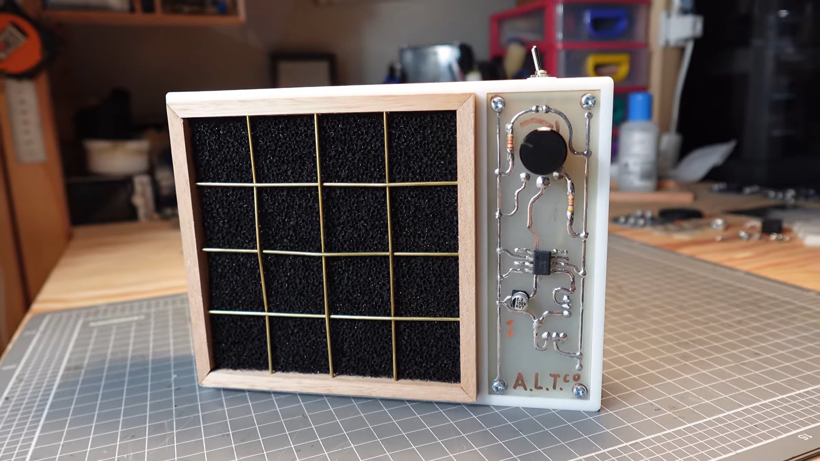
[ALTco] starts by thoroughly cleaning a raw copper-clad board so the marker sticks properly, then draws the circuit for a little analog fan controller. The board is then laid in a bath of the etchant for several minutes while gently rocking it to keep the reaction going. Finally the board is taken out, etchant stored for re-use, and the board washed with water and then presumably IPA to remove the remaining marker. Some assembly of the newly-printed circuit board later and you have a cute little smoke absorber for your soldering projects.
This articles is written by : Nermeen Nabil Khear Abdelmalak
All rights reserved to : USAGOLDMIES . www.usagoldmines.com
You can Enjoy surfing our website categories and read more content in many fields you may like .
Why USAGoldMines ?
USAGoldMines is a comprehensive website offering the latest in financial, crypto, and technical news. With specialized sections for each category, it provides readers with up-to-date market insights, investment trends, and technological advancements, making it a valuable resource for investors and enthusiasts in the fast-paced financial world.