
Idea and system construction
Due to the cooling finances, solely a small variety of management/readout electronics can be found in cryostats. Due to this fact, not just for gadgets that amplify RF alerts, routing gadgets are crucial as effectively to manage/readout a lot of qubits with a small variety of cryogenic electronics. Determine 1b, c outlines the idea and construction of the gadgets. An III-V heterostructure and Nb superconductor are monolithically built-in on Si, and we used these supplies to manufacture gadgets for amplifier and routing circuit. The strategies for the monolithic integration of various supplies into Si are totally defined in Supplementary Fig. 1, 2 and Strategies. By using III–V on Si know-how by way of wafer bonding, even RF circuits will be carried out23,24. The system for RF sign amplifier consists of a HEMT with scaled T-gate (Fig. 1d) and an Nb-based superconductor (Fig. 1e). Among the many huge number of superconductors, Nb was chosen as a result of its superconducting properties at 4 Ok and its glorious compatibility with III–V supplies, particularly InGaAs, when it comes to contact resistance (Supplementary Fig. 3). Moreover, the Nb and InGaAs contact is predicted to exhibit glorious system reliability as a result of its non-alloyed nature25,26. Just lately, analysis has progressed in the direction of epitaxially rising Nb on III–V supplies27, additional increasing its potential throughout quantum computing functions. The routing circuit additionally consists of III–V HEMT and Nb superconductor, however the important thing design strategy utilizing III–V 2DEG native interconnect and Nb world interconnect is utilized. The III–V 2DEG is used for transistor-to-transistor connections (known as native interconnect) to eradicate the vertical transport resistance, which is the principle bottleneck at cryogenic temperatures, resulting in extraordinarily low resistance and excessive scalability. Furthermore, for the worldwide interconnect, the Nb superconducting materials is used to successfully take away the parasitic resistance, leading to low-noise and low-power operation (Fig. 1f).
The next dialogue particulars how the cautious design of III–V heterostructure and the introduction of Nb superconductors appropriate for III–V supplies enabled the event of high-performance cryogenic gadgets. These gadgets function at 4 Ok with high-frequency, low-noise, and low-power consumption, attaining a determine of advantage that considerably surpasses the present cutting-edge. This idea provides a promising route for future large-scale quantum computing programs.
Design and characterization of III–V heterostructure
III–V heterostructure needs to be rigorously designed for low-power and low-noise operation at cryogenic temperatures. HEMTs are constructed primarily based on heterojunctions of a number of III–V supplies. As a result of InAlAs/InGaAs heterojunction with Si delta doping, 2DEG is fashioned within the quantum effectively channel with very excessive electron mobility (40,000 cm2 V−1 s−1 at 4 Ok) (Fig. 2a). Nevertheless, a vertical transport resistance part is inevitably created within the barrier layer, which is named barrier resistance (Rbarrier). This part accounts for a big portion (about 60% or extra) of the entire resistance within the InGaAs HEMTs at room temperature28,29. Because the surroundings transitions to cryogenic circumstances, this part turns into extra dominant due to the change in main mechanism from thermionic emission to area emission (Fig. 2b). Notably, the extent of area emission is modulated by layer thickness. Consequently, optimizing barrier thickness is crucial for the minimization of the Rbarrier.

a Schematic of the III–V heterostructure on Si with Al2O3 bonding dielectric and SiO2 interlayer dielectric. b Illustration of the conduction band of III–V heterostructure alongside the road AB in (a). Two completely different emission mechanisms (thermionic emission and area emission) are proven. At cryogenic temperatures, area emission is a dominant mechanism. c Three completely different III–V heterostructures with completely different barrier thicknesses. The InAlAs barrier thicknesses are 18, 11, and 9 nm, respectively, and all different layers are the identical. d R2DEG versus temperature for 3 completely different III-V heterostructures. e Rsh versus thickness at 4 Ok for III–V 2DEG and standard metallic (Al) and semiconductor (n+-Si). Rsh of III–V 2DEG is greater than 10 instances decrease than typical high-doped Si and similar to Al metallic of the identical thickness. f Dependence of Rbarrier on temperature in several III–V heterostructure. Because the temperature decreases, the distinction within the Rbarrier attributable to variations in barrier thickness will increase. This phenomenon is attributable to a change within the mechanism at cryogenic temperatures and underscores the essential function of barrier scaling at cryogenic temperatures.
To discover the sensible impression of barrier thickness on the traits of III–V heterostructure at cryogenic temperatures, we designed epitaxial buildings with barrier thicknesses of 18, 11, and 9 nm, whereas sustaining the opposite layers an identical, as proven in Fig. 2c. The cross-sectional scanning transmission electron microscopy picture of the three completely different III–V heterostructures will be present in Supplementary Fig. 4. The outcomes of the characterization are summarized in Fig. 2d–f. The sheet resistances of 2DEG (R2DEG) in our 3D built-in InGaAs HEMTs vary from 91 to 132 Ω sq-1 at 4 Ok, which is barely greater than the R2DEG for state-of-the-art typical InGaAs HEMTs (20 to 90 Ω sq-1)20,25,30,31, primarily as a result of bottom interface, which requires additional research to mitigate its impression sooner or later. However, the R2DEG of 91 Ω sq-1 at 4 Ok is greater than 10 instances smaller than a typical high-doped Si semiconductor and an identical sheet resistance to Al metallic of the identical thickness. This is because of the truth that the electron mobility of 2DEG turns into greater at 4 Ok, which allows a better frequency, and decrease energy and noise operation. Nevertheless, the comparability of the Rbarrier as proven in Fig. 2f reveals that the excellent conductivity achieved by the InAlAs/InGaAs heterostructure with Si delta doping might be of little worth until the Rbarrier will be suppressed. For non-optimized barrier thickness resembling EPI-A as proven in Fig. 2c, the Rbarrier at 4 Ok will increase to over 1000 Ω μm, which is equal to the resistance of a ten μm lengthy channel on a 2DEG with a sheet resistance of 100 Ω sq-1. This demonstrates that the thickness of the InAlAs barrier has a dominant impact on Rbarrier and, consequently, performs an important function in figuring out the general system resistance at cryogenic temperature. Due to this fact, to make sure the efficient operation of a scaling system with a sub-micron stage, the Rbarrier should be lowered to roughly 100 Ω μm. The III–V heterostructure with the scaled InAlAs barrier of 9 nm exhibits very low Rbarrier values of 132 Ω μm. Such a low Rbarrier can play a key function in enabling high-frequency, low-noise, and low-power operation at cryogenic temperature. On this context, the barrier thickness performs a vital function. A scaling barrier thickness permits a simpler area emission, permitting the low parasitic resistance at cryogenic temperature. Nevertheless, over-scaling the barrier thickness may cause excessive gate leakage and generate further noise, so designing an acceptable barrier thickness is essential, and the 9 nm barrier was used on this research. The detailed system traits relying on the III–V heterostructure will be present in Supplementary Fig. 5.
Cryogenic system for low energy and low noise amplifier
The characterization of the III-V HEMT with Nb superconductor built-in on Si was carried out at 300 Ok and 4 Ok in a cryogenic probe station. The detailed measurement setup is described in Strategies. All the outcomes reported within the following confer with two-finger gadgets with gate size LG = 70 nm. For a good comparability, currents have been normalized by the entire width of the system. The switch traits at low drain voltage (VDS) of fifty and 100 mV are proven in Fig. 3a. When the temperature drops to cryogenic ranges, the subthreshold swing (SS) of the system is improved and the off-current of the system decreases together with the lowering gate leakage present (Supplementary Fig. 6). At 4 Ok, the minimal SS is 35 mV dec−1 at VDS = 50 mV, and the gate leakage present is within the order of 10-8 A μm−1 throughout typical optimum low-noise operation of gate voltage (VGS), which is sufficiently small to not dominate the noise efficiency. The SS worth of 35 mV dec-1 is just not exceptionally low in comparison with beforehand reported cryogenic gadgets20,21,32,33. That is attributed to fluctuations within the channel potential34,35, which affect the extent of dysfunction throughout the system, thereby impacting the SS of the system. This impact largely relies on the channel construction34,35, making the design of an acceptable channel construction necessary for quantum computing functions. Determine 3b presents the transconductance (gm) traits measured at VDS of fifty and 100 mV. A tremendously improved gm of 0.8 S mm-1 is obtained at 4 Ok with a low VDS of 100 mV in comparison with 300 Ok because of the elevated mobility and the lowered parasitic resistance obtained by the optimized III-V heterostructure and Nb-based contact (Supplementary Figs. 3, 7). The small parasitic resistance and glorious mobility traits at 4 Ok may also be discovered within the output traits of the system measured over VGS vary of −0.7 to 0.3 V with 0.1 V steps (Fig. 3c), exhibiting improved on-resistance (Ron) of 0.4 Ω mm and most drain present of 1225 mA mm-1 at VGS of 0.3 V at 4 Ok. The low noise potential of the system will be clearly seen in a determine of advantage known as the noise indication issue ((sqrt{{I}_{{{rm{D}}}}}, {g}_{{{{rm{m}}}}}^{-1})), which is especially necessary for low-noise and low-power RF functions36. The noise indication issue as a operate of ID is reported in Fig. 3d. At 4 Ok, the system displays a low noise indication issue of 0.21 (0.21sqrt{{{{rm{Vmm}}}}}scriptstylesqrt{{S}^{-1}}) at ID of 20 mA mm-1. The ID is a spread of 15–20 mA mm-1 for optimum low-noise operation, which is a really low present stage and due to this fact appropriate for low-power operation.
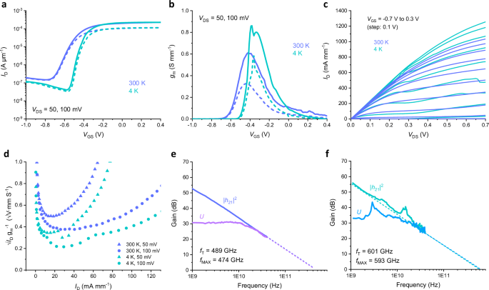
Switch (a) and transconductance (b) traits of III–V HEMTs on Si with LG of 70 nm and WG of two × 20 μm measured at VDS of fifty (dashed) and 100 mV (stable). The measurements have been carried out at 300 Ok and 4 Ok. When cooled to 4 Ok, the system displays switch traits with improved SS of 35 mV dec−1 at VDS = 50 mV. The constructive threshold voltage (VTH) shift can be noticed. The system provides sharper gm traits and a excessive peak gm of 0.8 S mm−1 at 4 Ok for a low VDS of 100 mV, in comparison with these noticed at 300 Ok. This enchancment at 4 Ok is attributed to enhanced 2DEG mobility and a discount in parasitic resistance. c Output traits of the identical system, exhibiting improved on-resistance and elevated most present at 4 Ok. d Noise indication issue versus ID of the system at a low VDS of fifty and 100 mV. The measurements have been carried out at 300 Ok and 4 Ok. The system exhibits a really low noise indication issue of 0.21 (0.21sqrt{{{{rm{Vmm}}}}}scriptstylesqrt{{S}^{-1}}) and the PDC at minimal noise indication issue is simply 0.8 and a couple of mW mm−1 at VDS = 50 and 100 mV. Acquire plots of III–V HEMTs on Si with LG of 70 nm and WG of two × 20 μm measured at 300 Ok (e) and 4 Ok (f). The measurements have been carried out at VDS of 500 mV and the optimum VGS for every temperature. The fT and fMAX are extracted by extrapolating the h21 and U curves with −20 dB dec−1 strains.
Excessive-frequency characterization was additionally carried out at each 300 Ok and 4 Ok utilizing vector community evaluation (VNA). Previous to system characterization, on-wafer calibrations have been carried out to take away extrinsic results from cables and probe station, making certain exact outcomes. The parasitic elements associated to the contact pad have been additionally eliminated by way of a pad de-embedding course of utilizing open and quick take a look at patterns fabricated on the identical substrate. Following this, the scattering (S)-parameters of III–V HEMTs on Si have been measured. The present acquire (h21) and unilateral energy acquire (U) derived from the S-parameter are proven in Fig. 3e, f. The system displays fT of 489 GHz and fMAX of 474 GHz at 300 Ok. When the temperature drops to 4 Ok, the fT and fMAX are tremendously enhanced to 601 and 593 GHz at a low VDS of 0.5 V as a result of improved electron mobility and lowered parasitic resistance, as analyzed within the DC traits. These outcomes reveal that III–V HEMT on Si-based cryogenic RF transistors not solely outperform CMOS-based cryogenic RF transistors but additionally present aggressive efficiency when in comparison with typical III-V-based cryogenic RF transistors. Just lately, researchers have been exploring optimum barrier, spacer, and channel buildings to additional improve the 40 dB acquire and 1.4 Ok common noise temperature of state-of-the-art InGaAs HEMT LNAs for quantum computing functions37,38. Incorporating such optimized designs into this research might convey us a big step nearer to attaining large-scale quantum computing platforms. Furthermore, as a result of our system is built-in on Si, it will probably break the trade-off relationship between cryogenic efficiency and integration functionality noticed in typical gadgets. In actual fact, our system will be built-in into cryogenic CMOS chip together with digital blocks or qubit processors, and the potential of this strategy has been demonstrated in earlier research by way of the implementation of heterogeneous and monolithic 3D integration of III-V and CMOS applied sciences39,40.
Routing technique with low energy consumption
To implement large-scale quantum computing programs throughout the restricted energy finances of a cryostat, the event of cryogenic RF transistors that function at very low energy is essential. Nevertheless, merely decreasing the ability consumption of cryogenic RF gadgets could have limitations. Due to this fact, there was energetic growth of routing circuits designed to manage and readout a lot of qubits with a small variety of cryogenic gadgets. A routing circuit for large-scale quantum computing programs should meet a number of standards: low energy consumption, low noise, low insertion loss, and excessive isolation functionality. Cryogenic routing circuits have already been demonstrated utilizing varied applied sciences resembling CMOS and III–V41,42,43,44,45,46. Nevertheless, one of many limitations for typical routing circuits is their massive vertical transport resistance. The portion of the vertical transport resistance of the 1-to-8 routing circuit using state-of-the-art cryogenic CMOS (22 nm FDSOI) is about 80% (Supplementary Fig. 8). It implies that the vertical transport resistance is a major bottleneck within the routing circuits at cryogenic temperature. Due to this fact, decreasing the vertical transport resistance or ideally eradicating the vertical transport resistance is the principle key to creating extremely scalable routing circuits.
To interrupt this bottleneck, we designed the routing circuit utilizing III–V 2DEG native interconnect and Nb superconducting world interconnect (Fig. 4a). Extra detailed cross-sectional buildings of routing circuits will be present in Supplementary Fig. 8. By changing the native interconnect between transistors from metallic to 2DEG, the vertical transport resistance will be successfully eradicated (Supplementary Fig. 8). On the worldwide interconnect facet, superconducting Nb is used to reduce the ability consumed of electrodes and suppress the self-heating generated because of this. The superconductive transition of the Nb is depicted in Fig. 4b, occurring throughout the temperature vary of 8 Ok. The working temperature for the routing circuits is 4 Ok, at which the Nb world interconnect stays superconductive. The time-domain measurements are proven in Fig. 4c. Making use of a relentless voltage to the frequent port, on-state voltage to A1, off-state voltage to A2, and on-state voltage pulse to B1 causes present to stream by way of the corresponding Y11 output. Conversely, making use of the off-state voltage to A1, on-state voltage to A2, and on-state voltage pulse to B2 leads to present stream by way of the corresponding Y22 output. These present the right routing operation in 1-to-4 DC routing. The projected whole resistance of our strategy and standard CMOS strategy for a similar structure is reported in Fig. 4d. The structure used for the prediction will be present in Supplementary Fig. 8. The routing circuits with 2DEG native interconnect and Nb world interconnect reveal roughly a 5-fold discount in resistance in comparison with the traditional construction in routing with 8 gates, and as much as roughly 10-fold reductions for 32 gates (Fig. 4d). The bigger the variety of gates, the larger the effectiveness of our construction, appropriate for large-scale quantum computing programs. This enchancment is attributed to the zero resistance of superconductive world interconnect and considerably lowered native resistance achieved by introducing 2DEG with out metallic contact between the channels. As the dimensions of the quantum laptop will increase, the impression of this construction turns into extra pronounced. Due to this fact, this structure might present a promising resolution for a extremely scalable routing system.

a Schematic of 1-to-4 DC routing circuit diagram. There are one enter and 4 outputs with 4 management gates (A1, A2, B1, B2). b Resistance of Nb versus temperature (normalized to the resistance at 10 Ok), exhibiting the transition temperature of 8 Ok. Inset consists of resistance values measured as much as 300 Ok. c Enter-output waveforms beneath completely different enter voltages, exhibiting the performance of the cryogenic routing. d Resistance benchmark for the introduced routing circuits in contrast with typical CMOS-based strategy (22 nm FDSOI) within the case of scaled construction. The structure of the routing circuit is present in Supplementary Fig. 8. The resistance is normalized to the resistance of a CMOS-based routing circuit with 32 gates. e Schematic of 1-to-2 RF routing circuit diagram. There are two RF output ports (RF1 and RF2) with one frequent port (RFC). The C1 and C2 are management gates. f S21 versus frequency beneath completely different Vov of the management gate. g Output waveform beneath completely different enter sign frequencies. h Output waveform for a 6 GHz enter sign with path 1 off and path B on. i Static energy consumption as a operate of Vov measured at 4 and 300 Ok. The road represents the standard operation area with a Vov vary of −0.1 to 0.4 V.
We developed not solely DC but additionally 1-to-2 RF sign routing circuits. As introduced in Fig. 4e, the RF sign is utilized to a standard port and divided into two paths. The trail is selectively linked or remoted through the use of III–V 2DEG on Si. By making use of bias on the management gate, the density of 2DEG is regulated, thereby altering the transmission of the RF sign (Fig. 4f). The insertion loss and isolation are 5.1 dB and 32.8 dB at 8 GHz. The switching ratio (S21,off – S21,on) is about 25 dB as much as 14 GHz, representing the appropriateness for management of spin qubits46. As proven in Fig. 4g, h, the time-domain response of the routing circuit is demonstrated by sign generator and oscilloscope. The routing circuit is just not considerably affected by frequency adjustments within the frequency vary of two–14 GHz (Fig. 4g) and demonstrates glorious routing capabilities (Fig. 4h). The static energy consumption, which accounts for many of the energy consumption of the RF routing circuit, is measured (Fig. 4i). As a result of lowered gate leakage at cryogenic temperatures, the swap can function with much less static energy consumption. Within the working vary of the swap (Vov: −0.1 to 0.4 V), it has a low energy consumption of as much as 60.8 nW per swap.
Efficiency benchmark
For cryogenic gadgets utilized in large-scale quantum computing functions, high-frequency, low-noise, and low-power traits are of main significance. The trade-off between excessive efficiency (excessive frequency, low noise, and low energy) and scalability (integration functionality and CMOS compatibility) is among the major limitations of typical cryogenic electronics. The state-of-the-art III–V HEMT-based cryogenic electronics, that are extensively utilized in at present’s quantum computing system, exhibit excessive cutoff frequency, low noise, and low energy consumption. Nevertheless, they aren’t thought of promising candidates for future large-scale quantum computing as a result of poor scalability and low compatibility with CMOS. Then again, CMOS-based cryogenic gadgets are very efficient from a scalability perspective as a result of energetic growth of CMOS-based spin qubits and the potential for CMOS to allow the co-integration of qubit-control/readout electronics. Nevertheless, they’ve the downside of being troublesome to realize excessive efficiency. Determine 5a, b present the efficiency benchmarking of the III-V-on-Si-based cryogenic RF electronics in contrast with different approaches together with III–V and CMOS which might be accessible within the literatures. The fT and (sqrt{{I}_{{{rm{D}}}}}, {g}_{{{{rm{m}}}}}^{-1}) are extracted at their respective optimum bias level. For our system, fT is extracted at VDS of 500 mV and (sqrt{{I}_{{{rm{D}}}}}, {g}_{{{{rm{m}}}}}^{-1}) is extracted at VDS of 100 mV. This benchmark highlights two main features of our gadgets. First, our III-V-based gadgets built-in on Si considerably outperform CMOS-based cryogenic gadgets. The cutoff frequency is about twice as massive, and the noise indication issue is roughly 15 to twenty instances smaller (Fig. 5a). It’s significantly necessary that these glorious traits are achievable at energy consumption greater than 10 instances decrease. Second, our system not solely surpasses CMOS efficiency but additionally demonstrates enhanced efficiency in comparison with beforehand reported III–V gadgets18,20,21,47,48,49,50. This vital enchancment might come up from two major elements: (1) optimized III-V heterostructure with QW channel and barrier thickness, which might extra successfully improve the electron mobility and cut back the parasitic resistance at cryogenic temperature; (2) the Nb-based ohmic contact successfully reduces the contact resistance, which is extra significance in scaling RF gadgets, enhancing high-frequency, low-noise, low-power traits. After all, fT and noise indicator don’t immediately symbolize the acquire and minimal noise ranges in an LNA circuit, however it’s clear that our system has ample potential as a qubit sign readout system. In future research, a complete analysis of the minimal noise after LNA fabrication might be crucial19,37,38.

fT versus (sqrt{{I}_{{{rm{D}}}}}, {g}_{{{{rm{m}}}}}^{-1}) (a) and fT versus PDC (b) benchmarks for state-of-the-art cryogenic RF transistors. The fT and (sqrt{{I}_{{{rm{D}}}}}, {g}_{{{{rm{m}}}}}^{-1}) are extracted at every optimum bias level, not on the similar bias. Among the many introduced gadgets, our system is closest to the optimum nook area (highest fT and lowest noise indication issue & highest fT and lowest PDC). Inset consists of fT versus (sqrt{{I}_{{{rm{D}}}}}, {g}_{{{{rm{m}}}}}^{-1}) benchmark just for III-V. Knowledge from refs. 18,20,21,47,48,49,50. c Projected energy consumption profiles for our system and CMOS relying on the variety of gates and contemplating the presence or absence of routing circuits. The routing ratio is 1-to-10. Coloured strains point out the cooling energy achievable with state-of-the-art dilution fridges, assuming 50% energy consumption on the readout.
Primarily based on the efficiency of cryogenic RF gadgets and routing circuits, we estimated the ability consumption of readout electronics. Determine 5c exhibits the projected energy consumption profiles for our proposed platform in comparison with a CMOS-only platform relying on the variety of gates and contemplating the presence or absence of routing circuits. Assumptions embody a routing ratio of 1-to-10 and 50% energy dissipation on the readout. Coloured strains symbolize the cooling energy offered by state-of-the-art dilution fridges. Our projections strongly reveal that: whereas utilizing solely CMOS know-how to manage and readout 1000’s of qubits is a sensible strategy, reaching tens of 1000’s of qubits or extra possible necessitates the implementation of III–V-on-Si know-how introduced by this work.
Now we have demonstrated cryogenic electronics utilizing III–V heterostructure and Nb superconductor, built-in on Si, for amplifying GHz vary sign and sign routing. The capabilities and benefits of our gadgets consequence from the distinctive mixture of a rigorously designed III–V heterostructure and the introduction of the Nb superconductor, offering state-of-the-art cryogenic efficiency. Crucially, as a result of our gadgets have been demonstrated on a Si wafer utilizing a heterogeneous and monolithic 3D integration methodology, it challenges the basic downside of typical III–V know-how, which is problem in integration with Si, thereby providing a path to extremely scalable quantum computing programs. Given the effectiveness of our heterogeneous and monolithic 3D integration resolution in accommodating a number of functionalities with out efficiency degradation39, extra functionalities resembling CMOS-based qubits (e.g., spin qubits) and management/readout electronics (e.g., analog-to-digital converters, digital-to-analog converters, and mixer) will be added to our strategy.
This articles is written by : Nermeen Nabil Khear Abdelmalak
All rights reserved to : USAGOLDMIES . www.usagoldmines.com
You can Enjoy surfing our website categories and read more content in many fields you may like .
Why USAGoldMines ?
USAGoldMines is a comprehensive website offering the latest in financial, crypto, and technical news. With specialized sections for each category, it provides readers with up-to-date market insights, investment trends, and technological advancements, making it a valuable resource for investors and enthusiasts in the fast-paced financial world.