

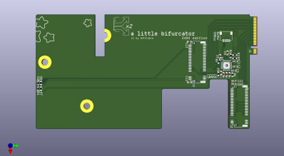
Today’s PCB design review is a board is from [Wificable]. iI’s a novel dual-SSD laptop adapter board! See, CPUs and chipsets often let you split wide PCIe links into multiple smaller width links. This board relies on a specific laptop with a specific CPU series, and a BIOS mod, to put two M.2 NVMe SSDs into a single SSD slot of a specific series’ laptop.
This board has two crucial factors – mechanical compatibility, and electrical function. Looking into mechanics, it’s a 0.8 mm thick PCB that plugs into a M.2 socket, and it has sockets for two SSDs on it – plenty of bending going on. For electronics, it has a PCIe REFCLK clock buffer, that [Wificable] found on Mouser – a must have for PCIe bifurcation, and a must-work for this board’s core! Apart from that, this is a 4-layer board, it basically has to be for diffpairs to work first-try.
Of course, the clock buffer chip is the main active component and the focus of the board, most likely mistakes will happen there – let’s look at the chip first.
All Eyes On Chip
The schematic is from a server board schematic – which is wonderful! Datasheet schematics are not always as complete or as succinct as you’d like them to be, and it’s super helpful to have a known-working schematic designed by a third party, that is production-grade and well-tested for 24/7 operation. We used that for our M.2 card design,
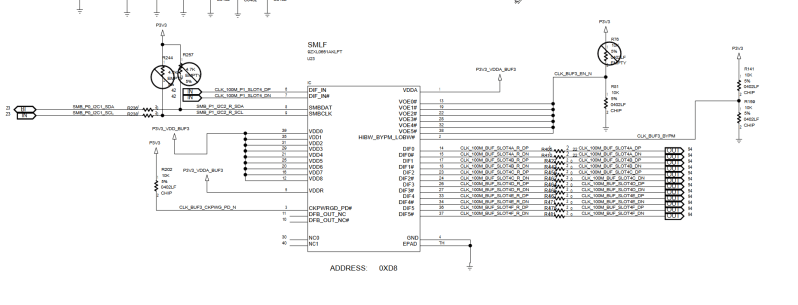
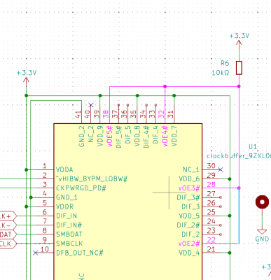
Of course, the symbol had to be redrawn for KiCad, and [Wificable] also rearranged the symbol corresponding to the physical pinout, as opposed to arranging them logically, like many KiCad symbols do. This is mostly a matter of preference and either way is fair – I switch between either of the two, depending on the situation. One note, though – when copying a schematic, I highly recommend you use the same pin arrangement as that schematic, it’s just really helpful to avoid mistakes.
In this case, I’d argue the logical arrangement is also cleaner, and that’s what I’d personally go for. However, design reviews are about function way more than aesthetics, and the chip’s wiring looked fine!
In my view, policing aesthetics is generally a no-go for PCB design – most you can do is suggestions. The line between aesthetic problems and practical problems is often blurry, let’s say, when the problem is about track routing, connector layout, making the schematic easy to check at a glance, or a good few other things. When in doubt, think about the best effort-to-payoff ratio for the person receiving the review.
Layout-wise, things are also fine – but they could be a little finer. The decoupling capacitors do need vias on their GND pads – easy to add, and a big benefit as far as power delivery goes. There are other areas where vias are called for! That, or having vias arranged a little differently, at the very least. Let’s take a look!
Well-Grounded
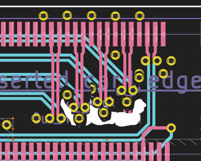
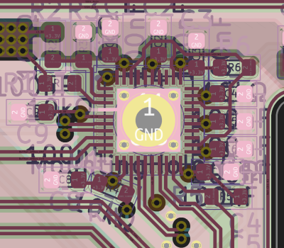
There are quite a few ground-related changes I’d recommend here specifically, given that it’s a high-speed design. I’ve been reading a fair few “how to treat ground fills better” documents, and they discuss about a row of signals with vias, ground unable to get between them. The recommended way is to arrange the vias diagonally, instead, letting some of the ground polygon fill between the gaps and freeing up space for GND vias – and that’s what we can do here, too.
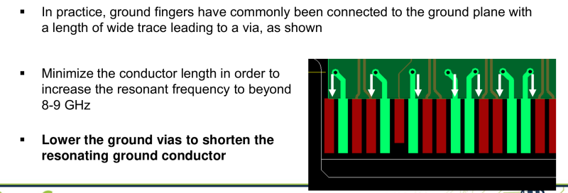
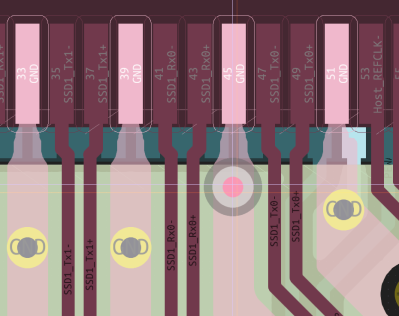
It’s also important to add vias on all GND pads next to high-speed signals, as close to the GND pads as possible. In our case, this means the M.2 edge and socket GND pads, so we have to move their respective GND vias as close to them as possible – signals have to be moved around a bit for this, but it’s worthwhile. Keep in mind – use the smallest vias your fab offers, at least without a price increase, because it helps a ton during design, especially considering how comically large the default KiCad vias are! The default is 0.8/0.4 (outer/drill), but you can safely go down to 0.6/0.4, and at fabs like JLCPCB, 0.5/0.3 is available without a price increase.
Do Not Bend
For dessert, we look at mechanics more closely. One thing that springs out to me – this is a 0.8 mm board inserted into a M.2 socket. The cutout in the middle is a liability. Some sort of cutout is necessary to accomodate plastic features of the laptop, but having a wide center-to-edge slot is a recipe for PCB bends. In this case, the edge-to-center slot can become a shorter one, mechanically connected on the edge again, just needs a little bit more measurement.
So far, the boards have been produced, thanks to Aisler’s new 0.8 mm four-layer process. They’ve been partially tested: [Wificable] didn’t get the chip yet, but has already successfully done the BIOS mod, and tested the bifurcation using magnet wire to switch between REFCLKs. Whenever [Wificable] finds time to finish testing, we will hear from her about how well the chip functions!
As usual, if you would like a design review for your board, submit a tip to us with [design review] in the title, linking to your board files. KiCad design files strongly preferred, both repository-stored files (GitHub/GitLab/etc) and shady Google Drive/Dropbox/etc .zip links are accepted.
This articles is written by : Nermeen Nabil Khear Abdelmalak
All rights reserved to : USAGOLDMIES . www.usagoldmines.com
You can Enjoy surfing our website categories and read more content in many fields you may like .
Why USAGoldMines ?
USAGoldMines is a comprehensive website offering the latest in financial, crypto, and technical news. With specialized sections for each category, it provides readers with up-to-date market insights, investment trends, and technological advancements, making it a valuable resource for investors and enthusiasts in the fast-paced financial world.