Many things about diamonds seem eternal, including the many engineering problems related to making them work as a silicon replacement in semiconductor technology. Yet much like a diamond exposed to a stream of oxygen-rich air and a roughly 750°C heat source, time will eventually erase all of them. As detailed in a recent [Asianometry] video, over the decades the challenges with creating diamond wafers and finding the right way to dope pure diamond have been slowly solved, even if some challenges still remain today.
Diamond is basically the exact opposite as silicon when it comes to suitability as a semiconductor material, with a large bandgap (5.5 eV vs the 1.2 of silicon), and excellent thermal conductivity characteristics. This means that diamond transistors are very reliable, albeit harder to switch, and heat produced during switching is rapidly carried away instead of risking a meltdown as with silicon semiconductors.
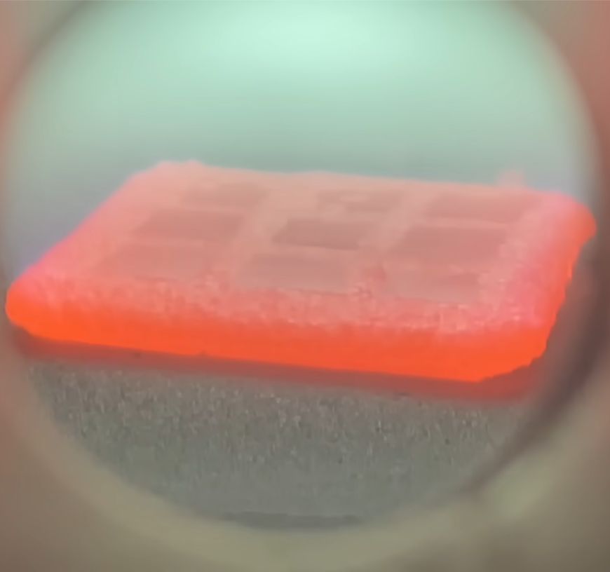
Unlike silicon, however, diamond is much harder to turn into wafers as you cannot simply melt graphite and draw perfectly crystallized diamond out of said molten puddle. The journey of getting to the state-of-the art soon-to-be-4″ wafers grown on iridium alongside the current mosaic method is a good indication of the complete pain in the neck that just this challenge already is.
Doping with silicon semiconductors is done using ion implantation, but diamond has to be special and cannot just have phosphorus and boron implanted like its sibling. The main challenge here is that of availability of charge carriers from this doping, with diamond greedily hanging on to these charge carriers unless you run the transistor at very high temperatures.
Since you can only add so much dopant to a material before it stops being that material, a more subtle solution was sought. At this point we know that ion implantation causes damage to the diamond lattice, so delta-doping – which sandwiches heavily doped diamond between non-doped diamond – was developed instead. This got P-type transistors using boron, but only after we pacified dangling carbon electron bonds with hydrogen atoms and later more stable oxygen.
State-of-the art switching with diamond transistors is currently done with MESFETs, which are metal-semiconductor field-effect transistors, and research is ongoing to improve the design. Much like with silicon carbide it can take a while before all the engineering and production scaling issues have been worked out. It’s quite possible that we’ll see diamond integrated into silicon semiconductors as heatsinks long before that.
Assuming we can make diamond work for semiconductor transistors, it should allow us to pack more and smaller transistors together than even before, opening up many options that are not possible with silicon, especially in more hostile environments like space.
This articles is written by : Nermeen Nabil Khear Abdelmalak
All rights reserved to : USAGOLDMIES . www.usagoldmines.com
You can Enjoy surfing our website categories and read more content in many fields you may like .
Why USAGoldMines ?
USAGoldMines is a comprehensive website offering the latest in financial, crypto, and technical news. With specialized sections for each category, it provides readers with up-to-date market insights, investment trends, and technological advancements, making it a valuable resource for investors and enthusiasts in the fast-paced financial world.